Research Activities on Nanoelectronics, Nanofabrication and Nanolithography
Research members: Jun-ichi Shirakashi PhD.
Research fields: Nano/Micro science, Applied physics, Electrical and electronic engineering, Material engineering
Departments: Institute of Engineering
Keywords: Single-Electron Transistor, Ultra-Small Tunnel Junction, Quantum Point Contact, Nanogap, Controlled Electromigration, Scanning Probe Microscopy, Electron-Beam Lithography
Web site:
Summary
OUR GROUP'S RESEARCH:
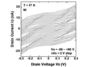
Focuses on the fabrication of nanodevices and measurement of their electronic and magnetic properties at low to room temperatures, and includes new nanofabrication techniques, magnetoresistance properties in ferromagnetic nanodevices and transport properties of electrons through Si and metallic/ferromagnetic nanostructures such as quantum dots and nanoconstrictions.
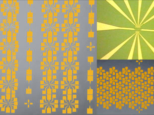
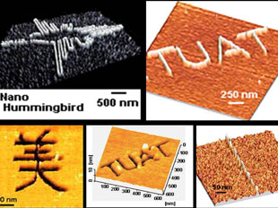
1) Nanofabrication: Scanning Probe Microscopy (SPM), Atomic Force Microscopy (AFM), SPM Local Oxidation Nanolithography, SPM Scratching Nanolithography, Electron-Beam Lithography.
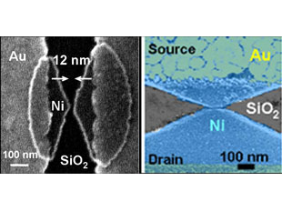
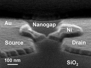
2) Nanodevices: Single-Electron Transistor (SET), Ferromagnetic Single-Electron Transistor (FMSET), Ultra-Small Tunnel Junction, Ferromagnetic Tunnel Junction, Quantum Point Contact (QPC), Ferromagnetic Nanostructure, Nanogap, Nanowire.
3) Physical Properties of Interest: Single-Electron Charging Effects, Controlled Electromigration Phenomena (Voltage-Controlled, Field-Emission-Induced, FPGA-Tuned, Real-Time-OS-Controlled), Resistive Switching Effects, Magnetoresistance (MR), Anisotropic Magnetoresistance (AMR), Tunnel Magnetoresistance (TMR), Domain Wall Magnetoresistance (DWMR), Spin Injection/Current Induced Magnetization Reversal.
Reference articles and patents
[1] R. Suda, M. Yagi, T. Watanabe and J. Shirakashi, "Formation Scheme of Quantum Point Contacts Based on Nanogaps Using Field-Emission-Induced Electromigration", J. Nanosci. Nanotechnol. 13 (2013) 883-887.
[2] S. Ueno, Y. Tomoda, W. Kume, M. Hanada, K. Takiya and J. Shirakashi, "Integration of Single-Electron Transistors Using Field-Emission-Induced Electromigration", J. Nanosci. Nanotechnol. 11 (2011) 6258-6261.
[3] T. Watanabe, K. Takiya and J. Shirakashi, "Fabrication of Planar-Type Ni/Vacuum/Ni Tunnel Junctions Based on Ferromagnetic Nanogaps Using Field-Emission-Induced Electromigration", J. Appl. Phys. 109 (2011) 07C919.
[4] W. Kume, Y. Tomoda, M. Hanada and J. Shirakashi, "Fabrication of Single-Electron Transistors Using Field-Emission-Induced Electromigration", J. Nanosci. Nanotechnol. 10 (2010) 7239-7243.
[5] J. Shirakashi, "Scanning Probe Microscope Lithography at the Micro- and Nano-Scales", J. Nanosci. Nanotechnol. 10 (2010) 4486-4494.
Contact
University Research Administration Center(URAC),
Tokyo University of Agriculture andTechnology
urac[at]ml.tuat.ac.jp
(Please replace [at] with @.)