ナノホールアレイ及びナノドットアレイの作製とデバイス応用
メンバー: 森下義隆
分野: プロセス・化学工学、材料工学、電気電子工学
所属: 工学研究院
キーワード: 陽極酸化、結晶成長、量子ドット、不揮発性メモリ
ウェブサイト:
研究概要
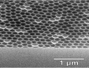
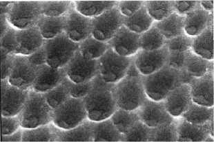
1. GaAsやInPなどの半導体基板の陽極酸化、またはGaAs基板に蒸着したAlの陽極酸化とGaAs基板へのパターン転写を用いて、半導体基板にナノホールアレイを作製し、孔に量子ドットを分子線エピタキシー成長し、位置とサイズの制御を行う。
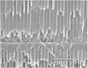
2. Aiシートの両面陽極酸化を行い、表面の孔と裏面の孔(または裏面の孔と孔の間の壁部分)で1対の抵抗可変型メモリ(ReRAM)の高密度作製を行う。
主要論文・参考事項
(1) Y.Morishita, T.Saito, and S.Kawai: Molecular-beam epitaxy of InAs on anodized GaAs substrates; J. Crystal Growth 201/202 (1999) 638-642.
(2)Y. Morishita,H、Yamamoto,and K. Yokobori: Electrochemical formation of GaAs honeycomb structure using fluoride-containing (NH4)2SO4 solution; Thin Solid Films 556 (2014)333-336.
お問い合わせ先
東京農工大学・先端産学連携研究推進センター
urac[at]ml.tuat.ac.jp([at]を@に変換してください)
Fabrication of nanosized-pore and/or -dot arrangements and their device application
Research members: Dr. Yoshitaka Morishita
Research fields: Process/Chemical engineering, Material engineering, Electrical and electronic engineering
Departments: Institute of Engineering
Keywords: Anodization, Crystal Growth, Quantum Dots, Nonvolatile Memory
Web site:
Summary
1. We attempt to establish a process technology for forming and transferring an arrangement of pore array on an Al film with the sizes and sites precisely controlled onto a GaAs substrate by 1) evaporating Al on the GaAs substrate, 2) anodizing the Al film, 3) transferring the pore arrangements onto the GaAs substrate. After removing the Al film, we grow InAs quantum dots only at the bottom of each holes formed on the GaAs substrate by molecular beam epitaxy.
2. Both sides of Al sheet are anodized: one-side of Al sheet is first anodized, and the pores are varied by metal, then the other side of Al sheet is anodized. After electrodes are formed on both sides of anodized porous alumina, resistive change random access memory (ReRAM) structure, consisting of a pair of pores formed on both sides or a pair of a pore of one side and oxide between pores on the other sides, is fabricated.
Reference articles and patents
(1) Y.Morishita, T.Saito, and S.Kawai: Molecular-beam epitaxy of InAs on anodized GaAs substrates; J. Crystal Growth 201/202 (1999) 638-642.
(2)Y. Morishita,H、Yamamoto,and K. Yokobori: Electrochemical formation of GaAs honeycomb structure using fluoride-containing (NH4)2SO4 solution; Thin Solid Films 556 (2014)333-336.
Contact
University Research Administration Center(URAC),
Tokyo University of Agriculture andTechnology
urac[at]ml.tuat.ac.jp
(Please replace [at] with @.)